Sustainable development triggers ultimate optimisation of materials on a nanoscale. The components must be localised in the correct place at the correct concentration in order to fulfill their function in the application. This creates a growing demand for methods capable of probing the molecular composition, at the surface and in-depth. A C60 sputter beam allows us to erode the material and analyse layers localised at the sub-µm scale.
The spectral information at each depth is stored and can be used for a depth profile or 3D reconstruction of the sample. Sputtering with C60 projectiles is still struggling with some bottlenecks such as sputter induced topography, anisotropic erosion and depth dependence of the SI yield.
In order to estimate the effect of these topics, atomic force microscopy (AFM) is used. AFM allows us to determine the erosion rate and the sputter-induced topography and finally optimise the 3D reconstruction.
Example: organic multilayers
Dual beam depth profiling and 3D analysis is a great tool for organic materials research. A bilayer of polyvinylpyrrolidone (PVP) and polymethylmethacrylate (PMMA), spincoated on a silicon wafer, has been used as a test system for the methodology.
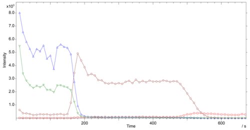
Analysis was performed on a ION TOF TOF-SIMS IV instrument with a Bi3+ LMIG for analysis and a C60 gun for sputtering. Spectra or ion images were acquired from areas of typically 50 µm x 50 µm and sputtering was performed with C603+ scanned over a surface of 300 µm x 300 µm. The figure below shows the sputter depth profile generated from the test system. The signals related to PMMA (blue and green) initially decrease and reach a steady state until the interface between PMMA and PVP is reached. The PVP related signal (brown) shows enhancement just after the interface and will reach a steady state afterwards and finally drop at the PVP-Si interface.

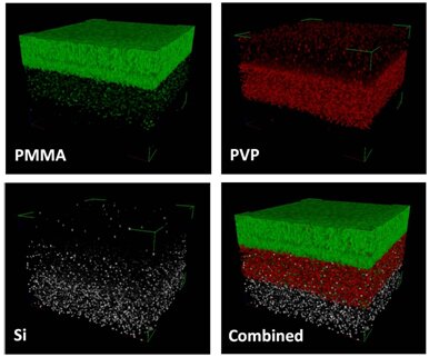
The 3D reconstruction of the test system is shown below. Traditional software stacks successive images at equal distances without accounting for the difference in sputter rate of different layers. This can result in incorrect layer thickness. Therefore a simple approach which takes into account the sputter rate has been developed. The software has stacked 34 SI images from the PVP layer at a certain distance followed by 17 SI image from the PMMA layer at a distance which is corrected for the ratio of the sputter rate of PVP and PMMA. The software allows to reconstruct flat organic multilayers with different sputter rates in 3D.
