Imaging in 3 dimensions
Modern TEM enables the investigation of nanostructures at the atomic scale. However, TEM images are only two-dimensional (2D) projections of a three-dimensional (3D) object. 3D imaging by TEM or "electron tomography" should be used to overcome this limitation. In conventional electron tomography, a tilt series of projection images (100-200) is acquired by tilting the sample over a large tilt range, with a tilt increment of typically 1 or 2º. After alignment of the projection images, using e.g. cross-correlation, the tilt series is combined into a 3D reconstruction of the original object through a mathematical algorithm. At EMAT, conventional tomography is used to investigate a broad range of (nano)materials in 3D. Typical examples of 3D reconstructions at the nanolevel are presented in Figure 1. The technique enables us to study the morphology and composition of nanoparticles and their assemblies, carbon nanotubes, porous materials, etc.
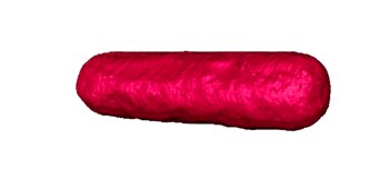
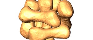
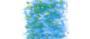
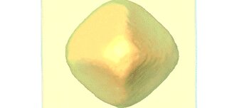
FIGURE LEGEND
3D visualisations of a) Morphology of a Au nanorod b) 3D stacking of an assembly of nanodumbbells, c) porous matrix containing catalytic particles d) Ag@Au core-shell particle.
In addition to application of electron tomography to a broad range of materials, it is also our goal to optimize the different steps in a tomography experiment. This is necessary since electron tomography is increasingly focused towards quantitative measurements. We therefore improve the acquisition of tilt series, the 3D reconstruction algorithms and the post processing procedures. In this manner, we are able to obtain quantitative measurements in 3D. Such measurements include porosity, particle diameter and distribution, chemical composition etc. Reaching atomic resolution in 3D has been the ultimate goal for many years. Although this is not yet a standard possibility for all structures, significant progress has recently been achieved by combining aberration corrected TEM with advanced computational methods.Examples are presented in Figure 2.
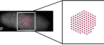
Clearly, advanced electron tomography will take characterization of nanomaterials to a new level. This will lead to a better understanding and optimization of existing materials as well as the design of new structures with desired properties. Although several nanomaterials have been visualised atom by atom, new challenges are currently emerging. One of these goals is to visualise defects or interfaces with the same resolution as demonstrated so far. Next, the aim will be to measure not only the positions of the atoms in 3D, but also to determine the chemical nature and oxidation state atom by atom.