EELS to the extreme
Electron energy loss spectroscopy (EELS) is based on the inelastic scattering of high energy electrons in materials. The energy loss of the primary electrons passing through the sample is measured by a spectrometer and is related to excitations of atoms in the crystal. EMAT has four microscopes with the latest EELS spectrometer technology (CM30, 3000F, Qu-Ant-Em, X-Ant-Em).
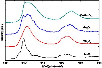
EELS is suited for the quantitative analysis of the elements Li to Np up to atomic resolution. The spectra can be quantified in terms of concentration of the elements with the help of the EELSMODEL software which was developed in EMAT. The detailed fine structure of EELS spectra (ELNES) can be related to the local valence, symmetry and magnetic state of specifically targeted atoms of a material. To interpret this information, comparison to either reference spectra (as shown in the first figure) or ab-initio (Computational Modeling of Materials) electronic structure calculations are needed. The spectral resolution is typically determined by the energy distribution of the electron source (typically 0.5eV) but can be dramatically improved (<0.15eV) by a monochromator as available on our flagship Qu-Ant-EM and X-Ant-EM microscope.
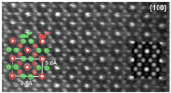
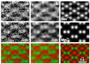
Combining these spectral capabilities with the latest state of the art in scanning finely focused electron probes over a sample (aberration corrected STEM, resolution down to 0.8 Å), leads to the amazing possibility of obtaining rich spectral data with atomic resolution. A dramatic example of this possibility is found in mapping the valence states in the mixed valence compound Mn3O4 . When viewing this crystal along a specific direction, different Mn atom sites in the crystal have a different ionic charge (or valence). This difference will lead to subtle changes in the fine structure of the EELS spectra which allows us to map the valence on an atom by atom basis (in TEM we always look at a projection through the sample, so it is better to say that we map atom column by atom column). The second and bottom figure show a summary of the experimental findings together with image simulations.
The importance of this capability can be understood for example as some recent nanoscale devices rely on the change of valence at an atomically sharp interface between two insulators to provide free electrons which create a two dimensional electrical transport layer. Other applications include the studying the catalytic activity of nanoparticles which often have a different valence at their surface as compared to the core of the particle.
As the interaction of a finely focused probe with matter allows for a complex interplay between inelastic and elastic scattering, it is sometimes far from trivial how to interpret the experimental results. In order to overcome this problem, we developed image simulation software that can simulate STEM EELS imaging at atomic resolution. This software also helps to decide which operation conditions to choose to optimize the experiment.
The improved energy resolution obtained with the use of a monochromator also makes EELS spectroscopy suitable for the study of nanoparticle based optical materials. Such materials have recently undergone a revival as it was shown that so-called surface plasmons in these materials can favorably enhance the efficiency of photovoltaic solar cells and light emitting diodes for lighting applications.
FIGURE LEGEND
A set of Mn L23 EELS spectra from different manganese oxides. Note the change in the detailed edge shape (ELNES) which can be used to probe the local electronic structure of a material.

HAADF STEM image of Mn3O4 indicating the different Mn cations in the structure.

Mapping of the two different Mn cations with atomic resolution based on the changes in ELNES fine structure. a) Raw data, b) low pass filtered and c) Inelastic image simmulation. This image shows that electronic structure information can be combined with atomic resolution in the latest state of the art electron microscopes as available in EMAT.
